nanoMETRONOM
Discover the world of nanoanalytics

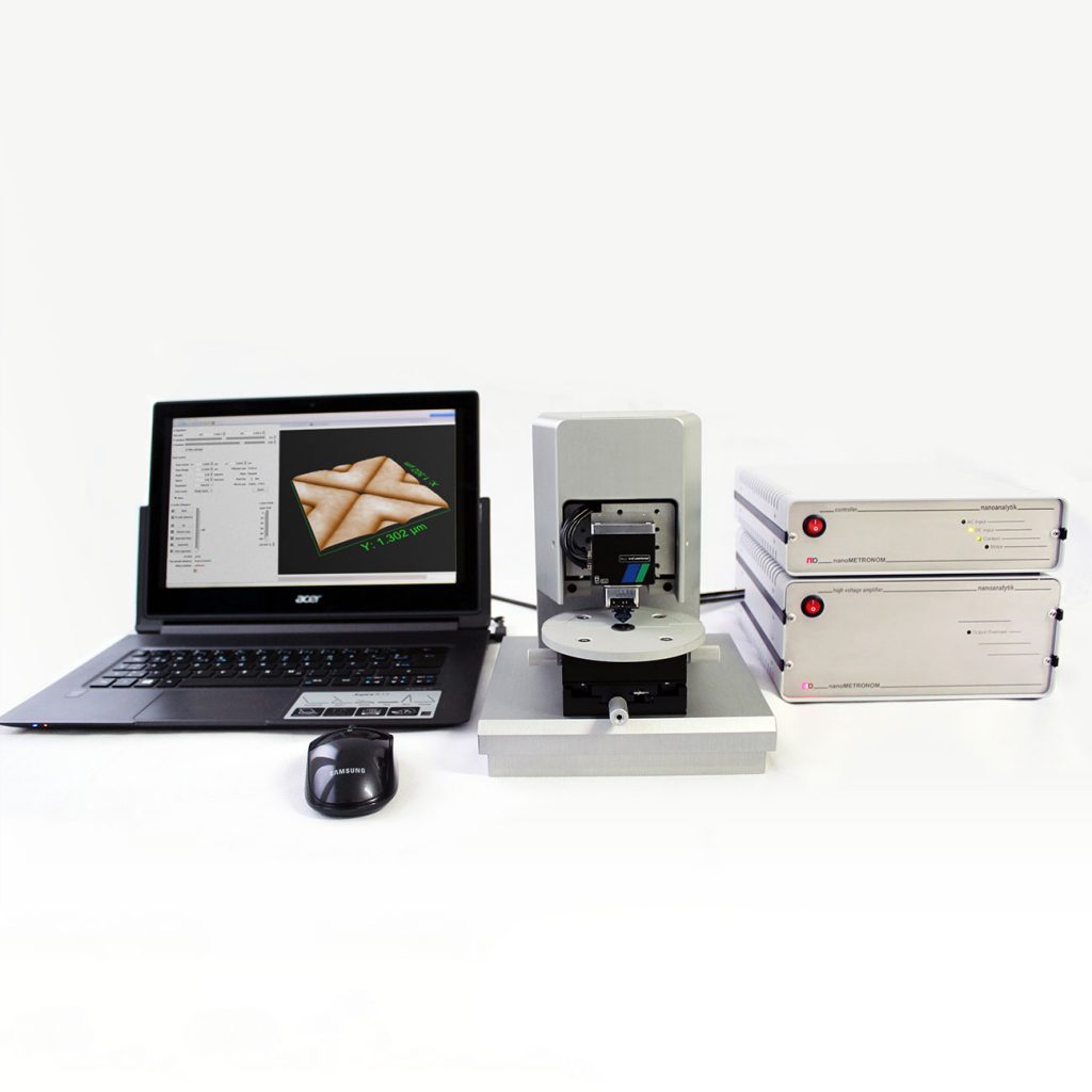
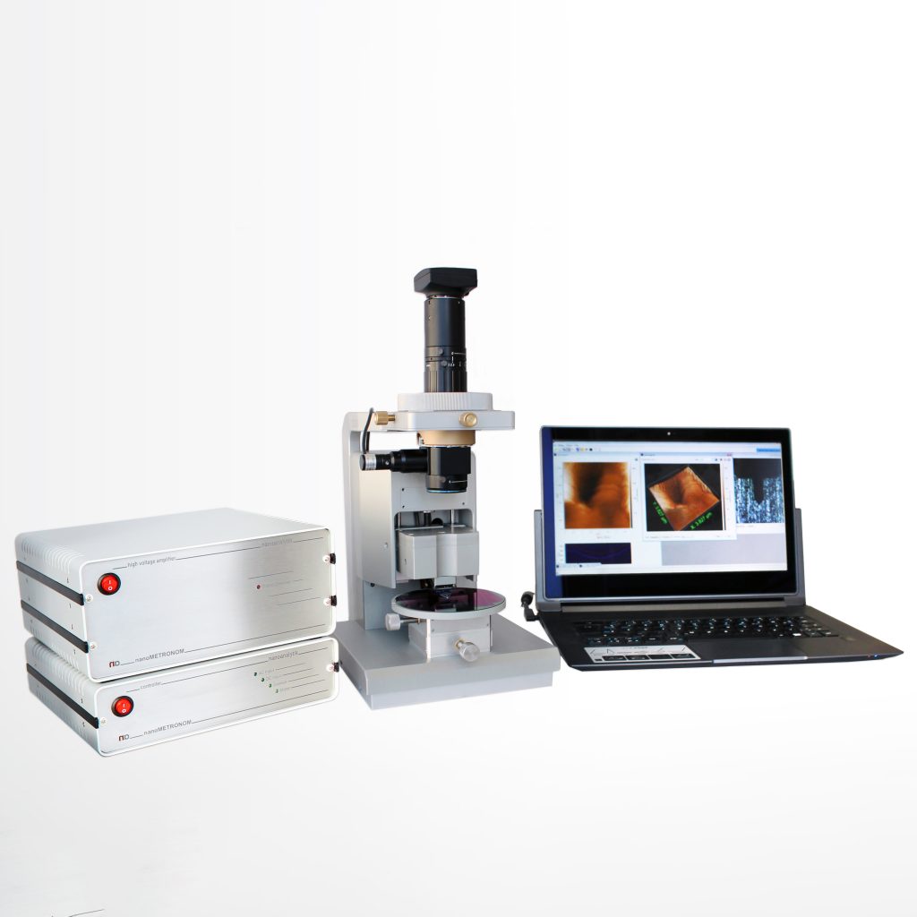
nano analytik GmbH offers this versatile, compact and extremely simple-to-use atomic force microscope (AFM) tool, allowing a huge variation of applications.
This novel nano analytik system has been developed in order to provide high-speed nano-scale imaging by “non-optical”, so called “active” cantilevers.
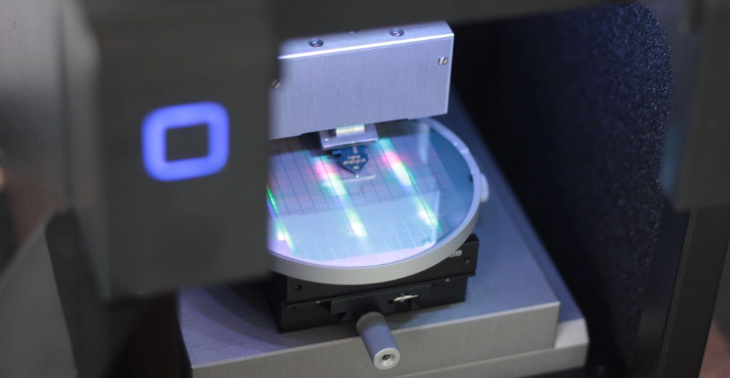
These cantilevers have an integrated piezo-resistive bridge sensor and thermomechanical actuator, making the necessity of complex manual AFM laser adjustments redundant. In particular, this system is very well suited for operation in vacuum in the fields of Materials Science applications.
It can be easily employed for e.g. chemical or bio-sensing, making it the first characterization system that allows investigation and calibration of diverse piezoresistive or capacitive cantilevers.
The nanoMETRONOM system has been developed to be a user-friendly nano-tech tool with an open modular architecture, making this remarkable instrument easy to be extended or modified on customer demand.
The key design and performance elements of nanoMETRONOM:
- For to industrial and academic research for complex nano-surface analysis
- Easy to use for unsurpassed usability
- Robust and reliable with high level automation
- Ultimately simple cantilever exchange “plug and play”
- High level automation for unsurpassed usability
- Diverse applications in materials science, semiconductors, mask-less lithography, thin films, soft polymers, coatings, hard metallic and ceramic systems, and bio-application
Specifications
| In-Situ Capability | Liquids, Gases. |
| Imaging Modes | Non-contact (Topography, Phase Shift, Error Signal), Contact-Mode & Force-Distance Curve. Other modes (C-AFM, KPFM, MFM, Lithography, SSRM etc.) upon request. |
| Channels | 2 |
| Digital Resolution | 18Bit (real noise-free resolution) |
| Controller Bandwidth | min. 5MHz |
| Scanner | Top-Scanner equipped with piezoresistive position sensors. Bottom-scanner arrangement possible as well. |
| Positioning Resolution | Closed-Loop X: 1nm, Y: 1nm, Z: 0.3nm; Open-Loop at least 5 times higher |
| Motionrange (X, Y, Z) | 35µm x 35µm x 10µm. Alternative: 100µm x 100µm x 30µm. Others on request. |
| Bottom Coarse Positioner | Typically manual micropositioner, motorized positioning stages on customer request. Travel range (X & Y) min. 10mm. Equipped with holder for 4 inch wafer. Customized holders for special purposes are possible as well. |
| Camera & Optics | System is by default equipped with a USB camera for optical sample navigation and an optical setup to adjust camera zoom. 2µm lateral resolution. |
| Software | The nanoMETRONOM system comes with nano analytik's standard AFM software. Travel range (X & Y) min. 10mm. Equipped with holder for 4 inch wafer. Customized holders for special purposes are possible as well. |
| Active Vibration Isolation | An active vibration isolation stage is included. |
Gallery