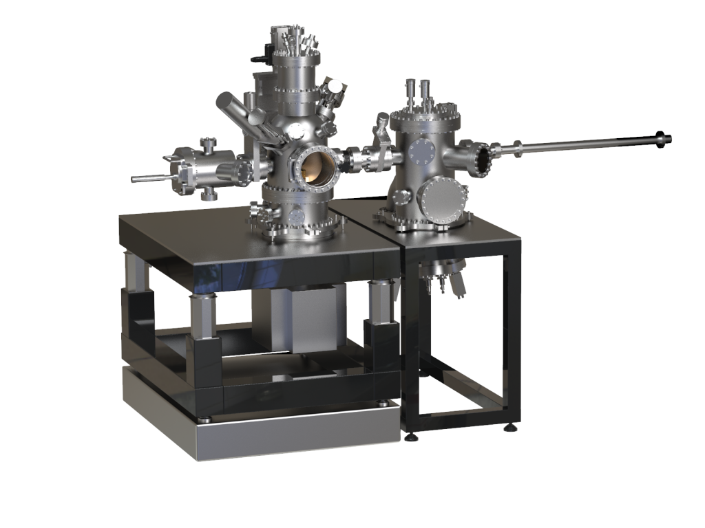
Multi-Plattform UHV System – AFM-MPS
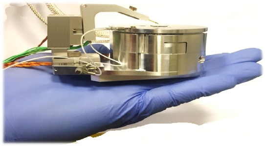
Atomic Force Microscope in a multi-instrument platform for nanoscale correlative fabrication and surface analysis.

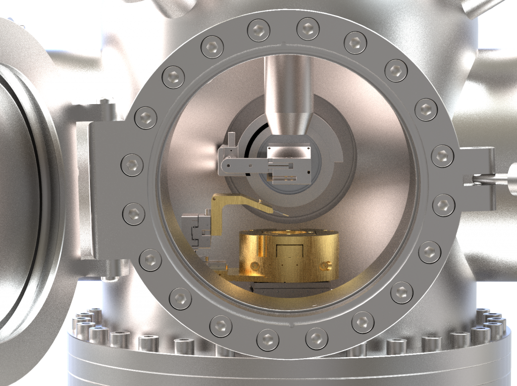
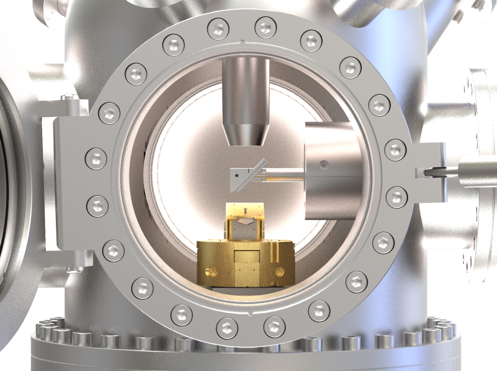
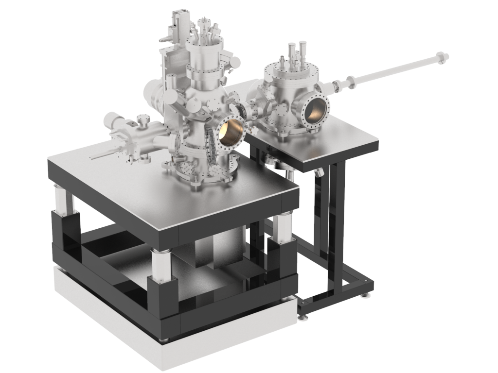
This multi technique design can combine AFM, AES, iXPS, one source for depth profiling, load-lock for transferring samples from/to the glove box under a protective atmosphere, and a second chamber (e.g. for magnetron coating or thermal evaporation). The primary, analytical chamber with AFM is mounted on the rigid frame put on the Gimbal Piston vibration isolation. If the vibrations in the lab are too high for passive vibration isolation, it is possible to mount the frame of the analytical chamber on an active vibration isolation floor platform or on active vibration isolation piezoelectric actuators, too. The second chamber can be mounted on a separate rigid frame. Both chambers can be connected by means of special flexible bellows that compensate for forces caused by pressure differences. The sample transfer rod can be mounted to the secondary chamber in order to minimize the vibrational influence on the primary chamber.
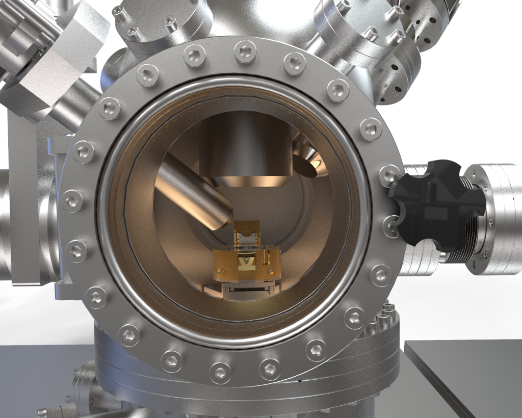
The sample size can be up to 2″.

Surface analysis methods:
- Atomic Force Microscopy (AFM) – ultra compact with active-cantilever
- Auger Electron Spectroscopy (AES)
- Photoelectron Spectroscopy using X-rays (XPS)
- Electron Energy Loss Spectroscopy (EELS) / REELS
- advanced optical imaging
- SEM imaging
- depth profiling
Correlative nanofabrication and surface modification:
- Single ion implantation (SII)
- Field emission scanning probe lithography (FE-SPL)
- Tip-based Electron Beam Induced Deposition (TB-EBID)
- PVD – thin-film deposition:
- sputtering
- thermal evaporation
Advantages:
- Large sample capability – sample diameter up to 2″
- The tool helps in the future development of the electronic devices based on single- or few dopant-QDs .
- In conventional EBID in the Scanning Electron Microscope (SEM), the primary electron beam (typically >500V) interacts with the substrate and generates backscattered electrons and low energy secondary electrons, which in combination determine the resolution.
- Based on a “top down” Field-Emission Scanning Probe Lithography (FE-SPL) approach, the realization of control gates and readout
SET structures becomes a realistic goal. - Our FE-SPL is used for fabrication of Single electron transistors (SETS), which make possible the control of quantum transport through ‘
a zero-dimensional island, source and drain, and gate electrodes. - Fast switching between electron-field emission from the tip and non-contact AFM imaging greatly facilitates analysis of the deposits. A
further important advantage is that the placement of the deposits is determined with very high positioning accuracy using the AFM f ·
navigation and fabrication of the EBID features.
Technical specifications of the AFM-MPS
AES/XPS analyser – DESA 150 from Staib Instruments
- Resolution at 1000 eV dE: less than 1 eV (On elastic peak at 1keV, FWHM)
- Resolution XPS: XPS (300W Mg, Ag 3d 5/2) less than 0.89 eV (FWHM)
- Signal to noise ratio AUGER on silver: Pulse counting – 600:1 or better
- Working modes: Constant Energy Resolution and Constant Resolution Ratio
- Energy range: 0 eV to 2500 eV
- Acceptance angle: 6% of 2Π
- Detection: Channeltron type electron multiplier
- Integrated electron source -Model EK-5IK
- Beam energy: 20 eV to 5 keV
- Minimum Spot size at 5 keV: < 100 μm, at 5 keV and low current
- Beam current max.: 20 μA
- Filament: Tungsten hairpin
- Scanning plates
- Source control – NEK-050
- Scannable beam
- Scan control (option): Scanning or imaging package
- Detection mode options: Pulse counting mode
- Data acquisition: WinspectroS multitasking acquisition package for Windows 7, 8, 10, WinspectroS VAMAS conform data file AUGER and ELS, SEM Optional, SAM Optional, XPS, UPS Optional, ISS Optional, SEM / SAM Optional
DUO-5-S.C.
- for depth profiling or sample cleaning
- Ion sources manufactured by STAIB Instruments are compact, high performance instruments.
- Type: UHV compatible douplasmatron
- Energy range: 500 eV to 5 keV
- Minimum beam diameter: 50 μm (dep. on energy and distance)
- Working pressure (chamber): 6 x 10⁻⁸ – 1 x 10⁻⁵ mbar
- Working pressure (ion gun): 1 x 10⁻⁴ – 1 x 10⁻³ mbar
- Working distance: 10 – 125 mm
- Deflection in X, Y
- Bakeout temperature 200° C
- Filament: cold cathode
- Differential pumping
- Emission current control
- Gases: Argon, Xenon, O2, H2
X-Ray Source System
- Mg/Al dual anode X-ray source package
- Power: 300W
- Anode: Al / Mg
- Window: Al
- Water cooling Approx.: 3.5 l/minute
- Security: interlock High voltage and water cooling
- Differential pumping: Optional / pumps not included
- Cooling circuit: Suggested; including water cooler and flow switch
- Z Translator: 100 mm
- HV Unit: 120V or 240V 50/60H
- Emission control: 100V-240V 50/60Hz
AFM/SPL/SDL head
- Vacuum and atmospheric operation
- Fast sample approach
- XYZ Scanning Stage
- non-magnetic
- closed-loop
- Range: 60µm x 60µm x 20µm
- Position Noise: X,Y=0.4nm; Z=0.2nm
- Resonant frequencies: X,Y=750Hz; Z=2000Hz
- XYZ Positioner
- closed-loop
- Range: X,Y,Z=15mm
- Accuracy: 3nm
- Standard measurement techniques:
- Real Non-Contact AFM
- Contact AFM
- Phase Imaging AFM
- Intermittent Non-Contact AFM
- Conductive AFM
- I-V Spectroscopy
- Kelvin Probe Force Microscopy (KPFM)
- KPFM with High Voltage
- Scanning Capacitance Microscopy (SCM)
- Scanning Spreading Resistance Microscopy (SSRM)
Gallery