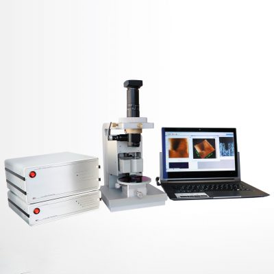
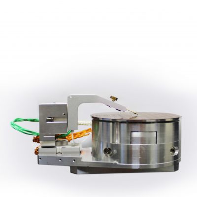
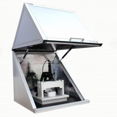
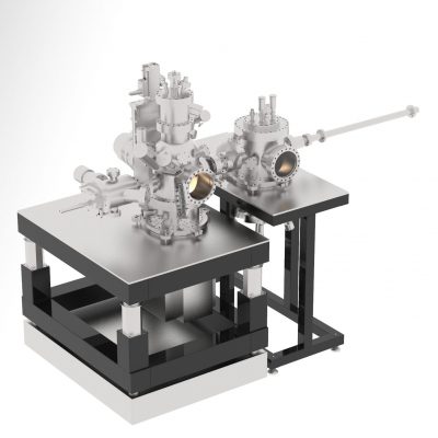
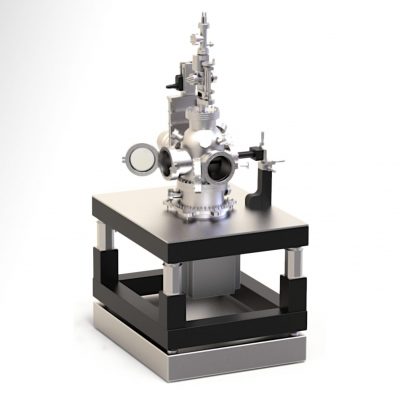
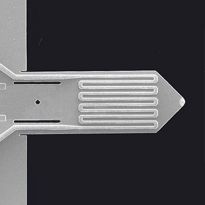
The AFM can be used for Tip-based Electron Beam Induced Deposition (TB-EBID) technique. This technique is using field-emitted low energy electrons (<75eV) emitted from the tip of an active cantilever. TB-EBID operates in the Single Digit Nanometer Regime and can be used for direct writing of nanostructures used for the fabrication of single-electron devices. The same tip is used for electron emission, AFM navigation and imaging.

Fast switching between electron-field emission from the tip and non-contact AFM imaging greatly facilitates analysis of the deposits. A further important advantage is that the placement of the deposits is determined with very high positioning accuracy using the AFM for navigation and fabrication of the EBID features.

