Single-Dopant Lithography – AFM-SDL
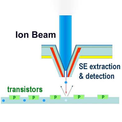
Combination of AFM and Ion Beam for Single Dopant Lithography.

The Atomic Force Microscope (AFM) is used as a tool for Single Dopant Lithography (SDL). SDL allows for generating features of single dopant atoms with high accuracy, such as Qbits, atomistic devices, and nitrogen-vacancy centers (N-V) in a diamond.
Enabling atomistic and quantum electronics
The future development of beyond-CMOS electronic devices is scheduled to be based on single- or few dopant-QDs. The capability to precisely position every single dopant atom is a fundamental step to enable the path to the future atomistic and quantum electronics. The development of an accessible quantum computer has emerged as a premiere challenge for the development of completely novel approaches in nanofabrication and nanotechnology in the last decade. Spins of electrons and nuclei of dopant atoms embedded in silicon are promising quantum qubit candidates.
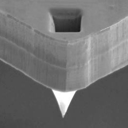
The integration of a scanning probe with an ion beam is similar to a “dynamic nano-stencil” for aligned placement of dopant atoms. The AFM provides high resolution, nondestructive imaging of the target and ensures precise navigation and positioning with sub-10nm resolution.
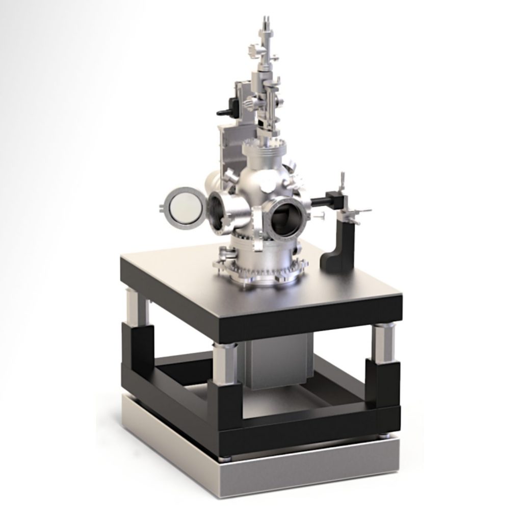
The heart of the SII tool is based on our compact AFMinSEM system that provides high speed non-contact imaging at atomic resolution under high-vacuum conditions. It is designed as an add-on module and can interoperate with a variety of different ion beam system, such as:
- focused ion beam systems (e.g. using liquid metal ion sources)
- rapidly emerging high-brightness ion sources (e.g. based on magneto-optical traps or on laser cooled ions)
- more conventional broad beam, relatively low-brightness ion source and beam transport systems
Donors can be placed in silicon or diamond.
In addition to SDL, the AFM-SDL100 system is capable of FE‑SPL and TB‑EBID. Thus, being able to create control gates and readout structures on its own, it paves the way towards fabrication of whole qubit arrays.
In summary, a versatile high-vacuum AFM system has been developed that can image at high speeds with atomic resolution without the need of external components. Here, the AFM-positioning accuracy and dynamic sub-5nm stencil functions can be combined with deterministic active substrate type single ion impact detection schemes and the ability to detect single ion impact and also, enables dopant implantation with impact detection integrated into the substrate This technique has been already implemented by several groups in Germany, USA and Australia [1].

| [1] |
|
Gallery